

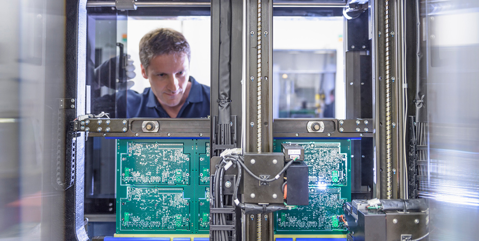
Bay Area Circuits provides bare board electrical testing to ensure that PCBs have been manufactured according to the design (Gerber, ODB++) files by testing for any shorts or opens. Testing is performed by flying probe machines, providing the fastest, most accurate test method for quick-turn prototypes and small to medium production.
Netlist
A netlist is recommended but not required for bare board testing. Upon beginning working on your order, Bay Area Circuits creates a netlist from the Gerber data, eliminating the need for a customer-provided netlist. But if a netlist was provided, the provided netlist is compared to the created netlist. Any discrepancies are resolved with the designer before proceeding. The netlist compare can and does catch very severe design errors but can only be done when a netlist is supplied.
Test Parameters
Standard test parameters are 100 V, 10 ohm continuity resistance, and 100 megaohm isolation resistance. High voltage testing and other custom parameters are available on request.
Verification
All boards that pass electrical test are stamped immediately after test to confirm the board has passed. The test stamp will typically go in an open area of the board, but if there is no space may be omitted or placed on the rails of an array. A designer may request no test stamp in the fab drawing notes.